I’m sure I’m not the only one who gets annoyed at long checkout queues and unnecessary delays when shopping. Recently I have been exploring the use of RFID tagging and other technologies to detect items and enable automated purchases. We are becoming more familiar with the use of smartphones for banking transactions via contactless (NFC) and being connected everywhere we go. All these technologies are coming together in ways that make our lives easier but at the same time it can be scary and leave us wondering if we are becoming too vulnerable to cyber crime.
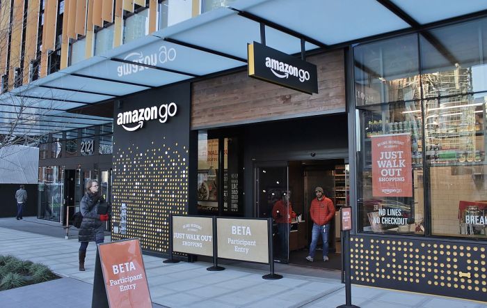
Amazon Technology are exploring ways of changing the shopping experience by trialing a “just walk out” system of shopping nicely explained in their video. I wanted to explore the technologies they were combining to enable this approach and found that a patent application filed about 4 years ago covers a range of the technologies they are testing in their Amazon Go stores. As usual the patent application is written in broad terms that can be adapted to a number of scenarios and so the terminology refers to a “material handling facility” rather than a shop.
Date: 8 Jan 2015
Inventors: PUERINI GIANNA LISE [US]; KUMAR DILIP [US]; KESSEL STEVEN [US]
Applicant: AMAZON TECH INC [US]
The description in the main body of the patent indicates that the technology can have application in stores, warehouses, libraries, museums, rental centres, etc.
Key enabling technologies are RFID tagging of items, image capture, facial recognition, sensors, wireless networks. Typical scenarios include a user entering a facility and being identified from a tag or smartphone device, selecting items and various methods are described for detecting when an item has been removed from a shelf and placed in a bag, a log of the items chosen is recorded and when the user exits the facility the transaction is completed – which can be that the user is charged for the items and the amount is deducted from their bank account.
It is possible to track the progress of this application in the Global Dossier and I can tell that the original claims have been rejected; revised claims have been submitted which seek to work around the objections made by the patent examiner.
Phil’s Comments
RFID technology is widely used as a tagging method and the cost per tag has come down dramatically in price through the developments in printed electronics. Direct printing of RFID on packaging is also possible. Reliable detection of passive RFID (no built in power source) is better than it was and so every item in a full bag of shopping can easily be detected as one passes a sensor. This application indicates that a whole range of technologies needs to work together seamlessly to get an automated shopping system working. The reliance on cameras to aid in the detection of users and items picked is actually higher than I expected, but is also reassuring in that it helps to increase security and offset the concerns that the system could be abused. The Amazon Go shop in Seattle has been running for about 5 months now but is only open to Amazon employees – I will keep an eye open for updates on its progress.
Please contact me if you would like more detailed patent analysis of this technology area.
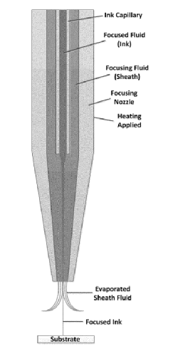 Summary: The present invention is directed to an apparatus for two-fluid hydrodynamic printing, comprising a coaxial tube assembly, comprising an inner tube having an exit orifice for flowing an ink stream therethrough and an annular outer tube for flowing a sheath fluid therethrough wherein the sheath fluid has a higher velocity than the ink stream such that the ink stream is hydrodynamically focused by the outer sheath fluid upon exiting from the exit orifice of the inner tube. The apparatus can further comprise a focusing nozzle downstream from the exit orifice of the inner tube for further focusing of the ink stream therein. The apparatus can further comprise means for removing the sheath fluid from the ink stream downstream from the exit orifice of the inner tube and a recirculation channel for recirculating the removed sheath fluid. For example the ink can comprise polyvinylpyrrolidone and the sheath fluid can comprise water, alcohol, or a combination thereof. The focused ink stream can be deposited on a substrate.


